|

|
|
|
|
|
|

|
제품에 대한 구입문의
또는 자세한 정보를
원하시는 분은 제품문의를
클릭하시고 내용을
입력해 주시면 빠른
시간 내에 답변드리도록
하겠습니다.
|
|
|
|
|
|
Si
Wafer
특성
|

|
|
|
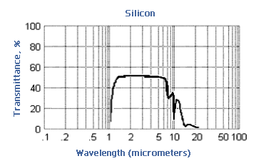
Silicon is commonly used as substrate material for infrared reflectors and windows in the 1.5 8 micron
region. The strong absorption band at 9 microns makes it unsuitable for CO2 laser transmission
applications, but it is requently used for laser mirrors because of its high thermal conductivity and
low density.
Silicon is also useful as a transmitter in the 20 micron range. Maximum available size: 102 mm Dia 50 mm Thk.
|
|
|
|
|
|
Chemical
Formula
|
Si
|
|
Molecular
Weight
|
28.09
|
|
Crystal
Class
|
Cubic
|
|
Lattice
Constant,
|
A 5.43
|
|
Density,
g/cm3
at
293
K
|
2.329
|
|
Dielectric
Constant
for
9.37
x
109
Hz
|
13
|
|
Melting
Point,
K
|
1690
|
|
Thermal
Conductivity,
W/(m
K)
at
125
K
at
313
K
at
400
K
|
598.6
163
105.1
|
|
Thermal
Expansion,
1/K
at
75
K
at
293
K
at
1400
K
|
-0.5
x
10E-6
2.6
x
10E-6
4.6
x
10E-6
|
|
Specific
Heat,
cal/(g
K)
at
298
K
at
1800
K
|
0.18
0.253
|
|
Debye
Temperature,
K
|
640
|
|
Bandgap,
eV
|
1.1
|
|
Solubility
in
water
|
None
|
|
Knoop
Hardness,
kg/mm2
|
1100
|
|
Mohs
Hardness
|
7
|
|
Young's
Modulus,
GPa
|
130.91
|
|
Shear
Modulus,
GPa
|
79.92
|
|
Bulk
Modulus,
GPa
|
101.97
|
|
Poisson's
Ratio3
|
0.28
|
|
|
|
|
Refractive
Index
|
|
Wavelength,
μm
|
1.40
|
1.50
|
1.66
|
1.82
|
2.05
|
2.50
|
3.50-5.00
|
6.00-25.00
|
|
Refractive
Index
|
3.49
|
3.48
|
3.47
|
3.46
|
3.45
|
3.44
|
3.43
|
3.42
|
|
|
|
|
|
|
|
|
|
|
|
|
|
|